Supports high aspect ratio structures up to 36.
Photodefinable polyimide material
◆Features
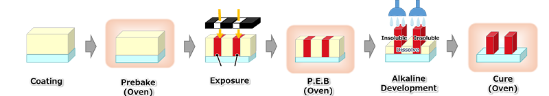
This is a negative-type photodefinable material that can be processed using photolithography, supporting film thicknesses up to 500 μm and aspect ratios up to 36. Taking advantage of the high reliability of polyimides (heat resistance, chemical resistance, mechanical strength, insulation, and X-ray resistance), we can expect their application in insulating materials for semiconductor/electronic components and structural materials for MEMS devices. We have newly developed STF-2000, a sustainable and eco-friendly product that is NMP-free, PFAS-free, and alkaline developable.
| Part No. |
STF-1000 |
STF-2000 |
| Features |
Capable of high aspect ratio patterning |
Environmentally friendly |
| Processed film thickness |
≦500μm |
≦200μm |
| Exposure wavelength |
h line (405nm) |
h line (405nm) |
| Development process |
Alkali development |
Alkali development |
| Contained solvent |
Non NMP solvent |
Non NMP solvent |
| PFAS free |
Not applicable |
Applicable |
| Storage conditions |
below -15℃ |
below -15℃ |
◆Processing method
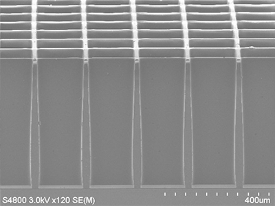
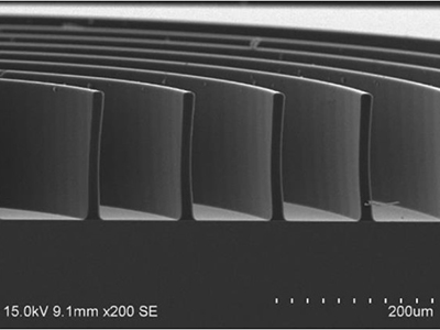
Example of processing (film thickness: 500 μm)
lattice (14 μm/160 μm)
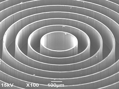
Example of processing (film thickness: 200 μm)
Coil shape (10 μm/100 μm)
Coil shape
 |
Cross section
➡⇩ |
 |
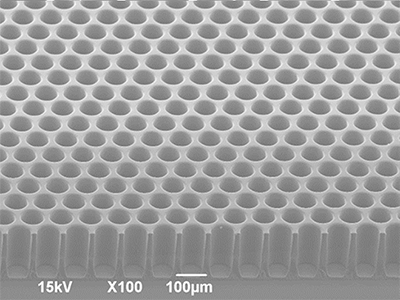
Via processing (Φ70 μm)
 |
Cross section
➡⇩ |
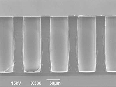 |
Line-and-space
 |
|
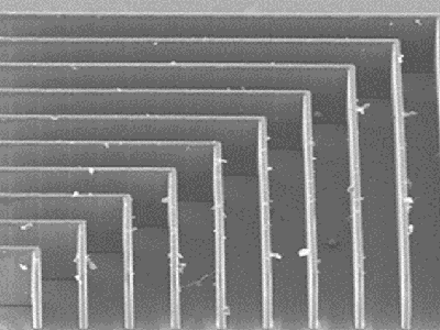
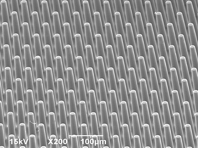
Pillar processing
 |
Physical properties of cured film (reference value)
| Part No. |
STF-1000 |
STF-2000 |
| Capable of high aspect ratio patterning |
Environmentally friendly |
| Glass transition temperature (℃) |
200~250 |
200~250 |
| 5% weight loss temperature (°C) |
280~330 |
280~330 |
| CTE(ppm/℃) |
70~75 |
70~75 |
| Elastic modulus (GPa) |
2.0~2.5 |
2.0~2.5 |
| Tensile strength (MPa) |
90~100 |
30~40 |
| Tensile elongation (%) |
6.0~8.0 |
1.5~2.5 |